

Go-X Series
CMOS area scan cameras that are compact, lightweight, and attractively-priced, with extra measures to prevent dust in the optical path.

Go Series
JAI's original small CMOS area scan cameras with 2.4 or 5.1 megapixel resolutions, three interface options, plus UV and polarized models.
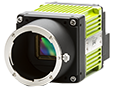
Spark Series
Advanced area scan cameras delivering high resolution, high frame rates, and high image quality.

Fusion Series
Multi-sensor area scan cameras with unique capabilities for multispectral imaging applications.
Fusion Flex-Eye
Custom-built multispectral cameras (visible and near-infrared light) with two or three sensors.

Apex Series
3-CMOS prism-based RGB area scan cameras providing better color fidelity than traditional Bayer cameras.

Apex Medical Solutions
The ultimate combination of color precision and dust-free image quality for medical and life sciences applications.

Sweep Series
Trilinear, bilinear and monochrome line scan cameras with fast scan rates and high image quality.
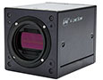
Sweep+ Series
Multi-sensor prism-based RGB, RGB/NIR and RGB/SWIR line scan cameras combining precision, sensitivity and multispectral options.
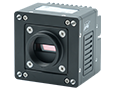
Wave Series
Single-sensor InGaAs area scan and line scan cameras for Short Wave InfraRed (SWIR) imaging.
Single-Sensor Color
A wide selection of color single-sensor area scan cameras with CMOS sensors including the latest Sony Pregius sensors. (Go-X Series, Go…

Single-Sensor Monochrome
A broad offering of monochrome single-sensor area scan cameras with CMOS sensors including the latest Sony Pregius sensors. (Go-X Series,…
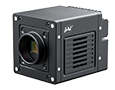
Single-Sensor SWIR
Single-sensor InGaAs area scan cameras for Short Wave InfraRed (SWIR) imaging.

Single-Sensor UV Sensitive
JAI offers several UV-sensitive area scan cameras to fit specific resolution, speed, and optical requirements. (Go Series)
2 and 3-Sensor Color + NIR (Prism)
JAI's multi-sensor, multispectral prism cameras provide simultaneous images of visible and NIR light spectrums through a single optical…
3-Sensor – R-G-B (Prism)
3-CMOS prism-based RGB area scan cameras provide better color fidelity than traditional Bayer cameras. (Apex Series and Apex Medical Series)

Single-Sensor Monochrome
Monochrome CMOS sensor line scan cameras with an excellent combination of high resolution and fast scan rates. Resolutions up to 8192…
Single-Sensor SWIR
Single-sensor InGaAs line scan cameras for Short Wave InfraRed (SWIR) imaging.
Trilinear and bilinear color
Trilinear and bilinear cameras deliver outstanding color line scan performance for applications that don't require the ultimate color…

2-Sensor SWIR+SWIR (Prism)
Prism based dual-sensor InGaAs line scan camera for Short Wave InfraRed (SWIR) light. (Sweep+ Series)

3-Sensor R-G-B (Prism)
3-sensor CMOS R-G-B color line scan cameras with state-of-the-art prism technology providing the best possible performance, precision, and…

4-Sensor R-G-B+NIR (Prism)
4-sensor line scan cameras designed to simultaneously capture R-G-B image data in the visible light spectrum and image data in the near…

4-Sensor R-G-B+SWIR (Prism)
4-sensor line scan cameras designed to simultaneously capture R-G-B image data in the visible light spectrum and image data in the short…